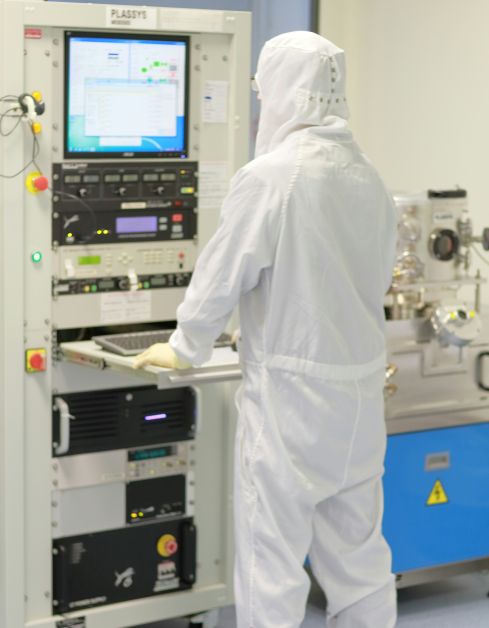
In order for AI to achieve balance with the environment, we must look at the environmental impact of the manufacturing process. While we read about net-gains towards the environment or reduction in energy and water requirements, that’s during live usage. It doesn’t factor the computer chip manufacturing process. I’ll describe that here.
Hybrid Chips – Next Gen
The next generation chips for AI will be a hybrid between both silicon and photonics. Let’s take a look at how this works.
- Silicon – Excels in complex logic, decision making and memory retention. However, moving electrons through copper wires creates a massive amount of resistance which generates the intense heat and energy waste.
- Photonics – Processes data with photons (light) traveling through microscopic etched channels (wave guides). Light waves do not interact or create friction so they generate virtually no heat. They travel at light speed and can run thousands of data streams simultaneously.
The Hybrid Chip
Both silicon and photonics sound great, but we need to dive a little deeper to understand why the hybrid approach is the better choice. Since this decision has already been made by the industry, we’ll look at the why then get into the manufacturing process itself.
- Memory problems – Photons move at the speed of light and cannot easily stop to store variables in memory. Silicon transistors, however, are perfect for holding data states.
- Manufacturing Maturity – Silicon manufacturing has been around a long time, is the most perfected, cost efficient supply chain. Photonic manufacturing requires specialized materials and incredibly precise packaging that is still scaling up in yield and standardization
- Photonics – These chips are incredible at something called matrix multiplication that drives deep learning and data routing, but they struggle with general purpose computing logic.
So we have silicon acting as the brains structure, and photonics acting like the nervous system and accelerator. AI training clusters utilizing this hybrid approach are already seeing energy efficiency gains of 70% to 90% per computation cycle.
Manufacturing Baseline
Now that we can see what needs to be done. creating these next generation computer chips, it’s time to look at what the environmental costs are.
- Silicon – Making a modern silicon GPU is an environmental nightmare. It requires ultra purified, massive amounts of water and extreme ultraviolet lithography machines that consumes megawatts of power 24/7
- Photonics – These chips will use silicon as a base, but they require additional exotic materials to generate and manipulate light.
- The Penalty – Manufacturing a hybrid photonic chip currently has a 1.5 to 2x higher carbon footprint at the factory level compared to a standard electronic chip because the manufacturing supply chain is still scaling up and maturing.
- Outlook – Through this process we’ll start with a net-negative to the environment with increased carbon debt.
Live Usage – Paying Back Debt
We have two parts to all computer chips. Manufacturing and running live. The manufacturing process will leave us with a net-negative impact to the environment through an increase in carbon debt. Live usage of these chips begins to pay back this debt.
- Silicon – In an AI data-center, roughly 40% of the total electricity doesn’t even go towards computing, it goes to massive air conditioning and liquid cleaning systems. Additionally, moving data between chips via copper wires accounts for 50% of a clusters energy use.
- Photonics – By replacing copper wires with light, data transmission energy drops by up to 80%. Heat generated drops so low that data-centers can drastically downsize their cooling infrastructure.
- Convergence – Because live usage accounts for roughly 80% to 90% of a chips total lifetime carbon footprint, the massive energy savings during operation rapidly pays back the higher carbon cost of manufacturing.
Problem and Sweet Spot
So we’ve decided on the next generation chip, identified the manufacturing and live usage costs to the environment and we come out with a net-gain towards the environment. Awesome, right? Wrong. We have a problem and it’s called The Jevons Paradox.
The Problem
Jevons Paradox – This paradox basically states that efficiency doesn’t always equal reduction. As a product becomes more efficient, people don’t use less of it, they actually use more.
As an example of Jevons Paradox within the field of AI, let’s look at radiology. AI helps radiologists review scans faster and more accurately. At first glance, you may suspect a decrease in the number of radiologists needed. The reality is the opposite. Lower costs and faster turnaround times, encourages more scans which in turn require more radiologists.
What all that means to our discussion above is simple. These more efficient, energy saving chips will increase demand and remove our net-positive gains to the environment.
The Sweet Spot
We can hit the net-positive environmental sweet spot between 2028 and 2032, driven by a three way convergence.
- Chip Tech – Hybrid silicon and photonic chips go mainstream slashing energy costs.
- Grid Power – Clean on-site microgrids roll out. Hyperscalers are investing in dedicated energy solutions so data-centers will run without touching the public grid.
- AI Software – Algorithmic efficiency. Software updates that require a fraction of the data to get the same results.
Warning: One thing to note is that changing the chip technologies alone will not get us to the sweet spot. It will certainly help to alleviate current pressures on the grid. The sweet spot comes when we achieve renewable microgrids and supply 100% clean energy directly to our data-centers.
Stop or Go
Manufacturing computer chips and expanding AI has become a hot topic. Some would insist we put on the brakes where-as others want to push ahead in a damn the torpedoes type of way. That’s two extremes and the answer lays somewhere in the middle. Let’s take a look.
Prisoners Dilemma
It’s best to show a chart explaining the prisoners dilemma.
| Company A Pauses | Company A Races | |
| Company B Pauses | Both build safe, green AI slowly. | Company B falls behind. Company A wins market dominance. |
| Company B Races | Company A falls behind. Company B wins market dominance. | Both build dangerous power-hungry AI, risking grid collapse. |
The Good and the Bad
- The Good – Collaborative Tech Roadmap. This initiative is backed by science as well as the tech community. The approach sets a hard, data-driven destination and gives science and industry the freedom to invent the path to get there.
- The Bad – Politics, plain and simple. Politicians don’t care about AI, they care about getting re-elected. This can drive them to do emotional driven things (think regulation and mandates or moratoriums)
Collaborative Tech Roadmap
A collaborative tech roadmap is a performance metric. Some governments want to ban data-centers based on size where-as science and industry are more interested in the reality of the numbers. While the government debates and writes papers, the science and technology communities have already begun to act.
Immediate Efficiency Floor By End of Year
- Rule – No data-center can be built unless its power usage effectiveness (PUA) is under 1.15. A value of 1.0 is perfect.
- Impact – This immediately outlaws old, inefficient architectures without stopping progress. It also mandates closed-loop water systems, meaning a data-center must recycle 95% of its own cooling water rather than evaporating millions of gallons into the air.
Infrastructure Transition Phase By 2028
- Rule – Any tech cluster expanding past a certain capacity must prove that 50% of its new energy load is coming from newly built, dedicated clean energy. This is a protective measure so the public grid isn’t being used.
- Photonic Mandate – Foundries must prove that any compound semiconductor chip contains standardized modular interconnects, allowing automated recycling machinery to easily separate the toxic optical components from the standard silicon at end-of-life.
Total Zero-Emission Independence By 2030
- Rule – All hyperscale AI data-centers must achieve 100% on-site, zero emission power generation and participate in a verified, closed-loop e-waste tracking program similar to the EU’s Digital Product Passport.
Politics
Why aren’t we doing this today? Politics. Science and technology moves at speeds far greater than the government. It’s easier for a government to pass sweeping legislation than to write highly technical, flexible regulations. In just a few pages the governments basically says stop building. It’s easier than trying to decide on the numbers provided above in the Collaborative Tech Roadmap outlined above. By the time the politicians finished such an exercise, the technology has already changed.
The good news is that the science and technology fields are already volunteering to follow where the science says it needs to go. Politics can be useful in these cases. Being voluntary now, governments can mandate and regulate. This basically does two things.
- Let science define the numbers that technology firms follow.
- Use the government as the hammer for any corporation found violating these numbers,.
Summary
We are currently going through the toughest times yet with regards to AI. We have a problem where our thirst for AI has outpaced our physical infrastructure. This doesn’t paint a dystopian narrative but it does call for the implementation of hybrid chip manufacturing and to closely follow the roadmap identified above. For more articles from me here at AI for the 21st Century, check out our AI and the Environment category.